
> GaN WaferPAM-XIAMEN specializes in GaN-based ultra high brightness blue and green light emitting diodes (LED)
and laser diodes (LD),also offer Gallium Nitride free-standing wafer and GaN Templates(GaN-on-sapphire).
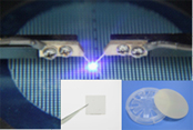
GaN on Al2O3-2” epi wafer Specification(LED Epiwafer)
|
White: 445~460 nm
|
|
Blue:465~475 nm
|
|
Green:510~530 nm
|
|
Structure layers
|
Thickness(μm)
|
|
p-GaN
|
0.2
|
|
p-AlGaN
|
0.03
|
|
InGaN/GaN(active area)
|
0.2
|
|
n-GaN
|
2.5
|
|
u- GaN
|
2
|
|
Al2O3 (Substrate)
|
430
|
|
Item
|
Color
|
Chip Size
|
Characteristics
|
Appearance
|
Application
|
|
|
|
|
|
|
Lighting
|
|
|
|
|
Vf = 2.8~3.4V
|
 |
LCD backlight
|
|
PAM1023A01
|
Blue
|
10mil x 23mil
|
Po = 18~25mW
|
Mobile appliances
|
|
|
|
|
|
Wd = 450~460nm
|
Consumer electronic
|
|
|
|
|
|
Vf = 2.8~3.4V
|
 |
General lighting
|
|
PAM454501
|
Blue
|
45mil x 45mil
|
Po = 250~300mW
|
LCD backlight
|
|
|
|
|
|
Wd = 450~460nm
|
Outdoor display
|
|
2" GaN Template
|
||
|
Item
|
PAM-GaNT-N
|
PAM-GaNT-SI
|
|
Conduction Type
|
N-type
|
Semi-insulating
|
|
Size
|
2"(50mm) dia.
|
|
|
Thickness
|
20um,30um
|
30um,90um
|
|
Orientation
|
C-axis(0001)+/-1°
|
|
|
Resistivity(300K)
|
<0.05Ω·cm
|
>1x10^6Ω·cm
|
|
Dislocation Density
|
<1x10^8cm²
|
|
|
Substrate Structure
|
Thick GaN on Sapphire(0001)
|
|
|
Surface Finish
|
Double Side Polished,epi-ready
|
|
|
Usable Area
|
≥ 90 %
|
|
|
Item
|
PAM-GaN50-N
|
PAM-GaN50-SI
|
|
Conduction Type
|
N-type
|
Semi-insulating
|
|
Size
|
2"(50mm) dia.
|
|
|
Thickness
|
230+/-20um, 280+/-20um
|
|
|
Orientation
|
C-axis(0001)+/-1°
|
|
|
Resistivity(300K)
|
<0.05Ω·cm
|
>1x10^6Ω·cm
|
|
Dislocation Density
|
<5x10^5cm²
|
|
|
Marco Defect Density
|
<5cm²
|
|
|
Surface Finish
|
Double Side Polished,RMS<2nm,N-Face RMS<1μm,epi-ready
|
|
|
Usable Area
|
≥ 90 %
|
|
|
10mm*10.5mm,GaN Free-standing Wafer
|
||
|
Item
|
PAM-GaN50-N
|
PAM-GaN50-SI
|
|
Conduction Type
|
N-type
|
Semi-insulating
|
|
Size
|
10mmx10.5mm
|
|
|
Thickness
|
230+/-20um, 280+/-20um
|
|
|
Orientation
|
C-axis(0001)+/-1°
|
|
|
Resistivity(300K)
|
<0.05Ω·cm
|
>1x10^6Ω·cm
|
|
Dislocation Density
|
<5x10^5cm²
|
|
|
Marco Defect Density
|
<5cm² or 5-10cm²
|
<5cm²
|
|
Surface Finish
|
Double Side Polished,RMS<2nm,N-Face RMS<1μm,epi-ready
|
|
|
Usable Area
|
≥ 90 %
|
|
|
*We also offer dia.45mm, dia 1", and 5mm*5mm,GaN Free-standing Wafer.
*We offer GaN free-standing LED grade and LD grade both.
* 5*5mm,10*10mm or custom size, GaN on sapphire,(0001), n type Si doped or undoped, 3-5um are available.
|
||
*For more information of GaN substrate, please see:Properties of GaN substrate