
> GaN substrate|
Item
|
undoped N-
|
Si doped N+
|
Semi-insulating
|
P+
|
|
Freestanding GaN substrate
|
yes
|
yes
|
yes
|
|
|
GaN on sapphire
|
yes
|
yes
|
yes
|
yes
|
|
InGaN on sapphire
|
|
yes
|
***
|
|
|
AlN on sapphire
|
|
|
yes
|
|
|
LED wafer
|
(p+GaN/MOW/N+GaN/N-AlGaN/N+GaN/N-GaN/sapphire)
|
|||
|
PROPERTY / MATERIAL
|
Cubic (Beta) GaN
|
Hexagonal (Alpha) GaN
|
|
.
|
.
|
.
|
|
Structure
|
Zinc Blende
|
Wurzite
|
|
Space Group
|
F bar4 3m
|
C46v ( = P63mc)
|
|
Stability
|
Meta-stable
|
Stable
|
|
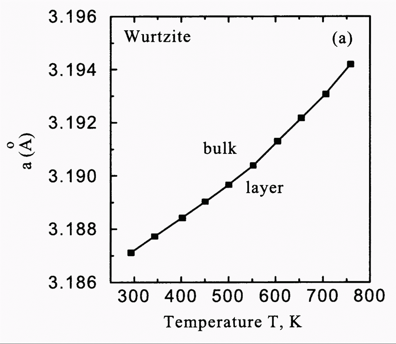
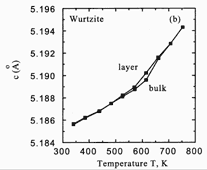
Lattice Parameter(s) at 300K
|
0.450 nm
|
a0 = 0.3189 nm
|
|
c0 = 0.5185 nm
|
||
|
Density at 300K
|
6.10 g.cm-3
|
6.095 g.cm-3
|
|
Elastic Moduli at 300 K
|
. . .
|
. . .
|
|
Linear Thermal Expansion Coeff.
|
. . .
|
Along a0: 5.59x10⁻⁶ K-1
|
|
at 300 K
|
Along c0: 7.75x10⁻⁶ K-1
|
|
|
Calculated Spontaneous Polarisations
|
Not Applicable
|
– 0.029 C m-2
|
|
Bernardini et al 1997
|
||
|
Bernardini & Fiorentini 1999
|
||
|
Calculated Piezo-electric Coefficients
|
Not Applicable
|
e33 = + 0.73 C m-2
|
|
e31 = – 0.49 C m-2
|
||
|
Bernardini et al 1997
|
||
|
Bernardini & Fiorentini 1999
|
||
|
|
|
A1(TO): 66.1 meV
|
|
|
|
E1(TO): 69.6 meV
|
|
Phonon Energies
|
TO: 68.9 meV
|
E2: 70.7 meV
|
|
|
LO: 91.8 meV
|
A1(LO): 91.2 meV
|
|
|
|
E1(LO): 92.1 meV
|
|
Debye Temperature
|
|
600K (estimated)
|
|
Slack, 1973
|
||
|
|
. . .
|
Units: Wcm-1K-1
|
|
|
|
|
|
|
1.3,
|
|
|
|
Tansley et al 1997b
|
|
|
|
|
|
|
|
2.2±0.2
|
|
|
|
for thick, free-standing GaN
|
|
|
|
Vaudo et al, 2000
|
|
|
|
|
|
|
|
2.1 (0.5)
|
|
|
|
for LEO material
|
|
|
|
where few (many) dislocations
|
|
|
Thermal Conductivity
|
Florescu et al, 2000, 2001
|
|
|
near 300K
|
|
|
|
|
circa 1.7 to 1.0
|
|
|
|
for n=1x10¹⁷ to 4x1018cm-3
|
|
|
|
in HVPE material
|
|
|
|
Florescu, Molnar et al, 2000
|
|
|
|
|
|
|
|
2.3 ± 0.1
|
|
|
|
in Fe-doped HVPE material
|
|
|
|
of ca. 2 x10⁸ ohm-cm,
|
|
|
|
& dislocation density ca. 105 cm-2
|
|
|
|
(effects of T & dislocation density also given).
|
|
|
|
Mion et al, 2006a, 2006b
|
|
|
|
|
|
|
Melting Point
|
. . .
|
. . .
|
|
Dielectric Constant
|
. . .
|
Along a0: 10.4
|
|
at Low/Lowish Frequency
|
Along c0: 9.5
|
|
|
Refractive Index
|
2.9 at 3eV
|
2.67 at 3.38eV
|
|
Tansley et al 1997b
|
Tansley et al 1997b
|
|
|
Nature of Energy Gap Eg
|
Direct
|
Direct
|
|
Energy Gap Eg at 1237K
|
|
2.73 eV
|
|
Ching-Hua Su et al, 2002
|
||
|
Energy Gap Eg at 293-1237 K
|
|
3.556 - 9.9x10⁻⁴T2 / (T+600) eV
|
|
Ching-Hua Su et al, 2002
|
||
|
Energy Gap Eg at 300 K
|
3.23 eV
|
3.44 eV
|
|
Ramirez-Flores et al 1994
|
Monemar 1974
|
|
|
.
|
.
|
|
|
3.25 eV
|
3.45 eV
|
|
|
Logothetidis et al 1994
|
Koide et al 1987
|
|
|
|
.
|
|
|
|
3.457 eV
|
|
|
|
Ching-Hua Su et al, 2002
|
|
|
Energy Gap Eg at ca. 0 K
|
3.30 eV
|
3.50 eV
|
|
Ramirez-Flores et al1994
|
Dingle et al 1971
|
|
|
Ploog et al 1995
|
Monemar 1974
|
|
|
Intrinsic Carrier Conc. at 300 K
|
. . .
|
. . .
|
|
Ionisation Energy of . . . Donor
|
. . . .
|
. . . .
|
|
Electron effective mass me* / m0
|
. . .
|
0.22
|
|
Moore et al, 2002
|
||
|
Electron Mobility at 300 K
|
. . .
|
.
|
|
for n = 1x1017 cm-3:
|
ca. 500 cm2V-1s-1
|
|
|
for n = 1x1018 cm-3:
|
ca. 240 cm2V-1s-1
|
|
|
for n = 1x1019 cm-3:
|
ca. 150 cm2V-1s-1
|
|
|
|
|
|
|
|
Rode & Gaskill, 1995
|
|
|
|
Tansley et al 1997a
|
|
|
Electron Mobility at 77 K
|
. . . .
|
. . . .
|
|
for n = . .
|
||
|
Ionisation Energy of Acceptors
|
. . .
|
Mg: 160 meV
|
|
Amano et al 1990
|
||
|
|
||
|
Mg: 171 meV
|
||
|
Zolper et al 1995
|
||
|
|
||
|
Ca: 169 meV
|
||
|
Zolper et al 1996
|
||
|
Hole Hall Mobility at 300 K
|
. . .
|
. . . .
|
|
for p= . . .
|
||
|
Hole Hall Mobility at 77 K
|
. . . .
|
. . .
|
|
for p= . . .
|
||
|
.
|
Cubic (Beta) GaN
|
Hexagonal (Alpha) GaN
|
Application of GaN substrate