
PAM-XIAMEN provide GaN/sapphire wafers as follows:
|
1 |
Description |
Maximum Permissible |
Inspection Level |
||||
|
1 |
Defects @ 50x |
|
per spec |
per 2" wafer |
|||
|
1.1 |
Voids |
0 |
per spec |
per 2" wafer |
|||
|
1.3 |
Large Defects |
0 |
per spec |
per 2" wafer |
|||
|
|
Large defects are defined as any defect >50um in width and >200nm in height. Large defects are visable to the naked eye under white light. |
||||||
|
1.4 |
Scratches |
edge ok |
per spec |
per 2" wafer |
|||
|
1.5 |
Contamination |
0 |
per spec |
per 2" wafer |
|
||
|
1.6 |
Defects (Particles, Pits) |
< 200 |
per spec |
per 2" wafer |
|||
|
|
Microscope images are taken from three locations: 1) 5mm from the top edge, 2) center of wafer and 3) 5mm from bottom flat. The total number of defects at these three location combined should be equal or less than 9 defects for the inspection to pass. |
||||||
|
2 |
Cracks |
0 |
count |
per 2" wafer |
|||
|
3 |
BOW |
< 50um |
per spec |
per 2" wafer |
|||
|
4 |
Resistivity |
< 20 milli-ohm cm |
per spec |
per 2" wafer |
|||
|
5 |
Surface Roughness |
< 12nm Ra (3 profilometer scans - 1mm length each) |
per spec |
per 2" wafer |
|||
|
6 |
Fishscale |
Not allowed |
per example |
per 2" wafer |
|||
|
2.Substrate spec |
For use with SSP |
|
|
2.10 |
Orientation: |
c-plane (0001) |
|
2.11 |
Offcut: |
0.2 +/- 0.1 degrees (M-plane) |
|
2.12 |
Diameter: |
2 inch (50.8 +/- 0.25mm) |
|
2.13 |
Thickness: |
430 +/- 20um |
|
2.14 |
Primary flat: |
16 +/- 1mm |
|
2.15 |
Flat location: |
A-plane (1120) +/- 0.3 degrees |
|
2.16 |
Front side finish: |
EPI Polish Ra <0.3nm |
|
2.17.1 |
Pattern Bottom Diameter: |
NA |
|
2.17.2 |
Pattern Pitch: |
NA |
|
2.17.3 |
Pattern Height: |
NA |
|
2.17.4 |
Pattern Type: |
NA |
|
2.18 |
Back side roughness |
Ra 1.0 +/- 0.5um |
|
2.19 |
Both sides beveled |
Rounded / Chamfering Angle (C) = 45° |
|
2.20 |
TTV |
<10um |
|
2.21 |
Bow |
<10um |
|
2.22 |
Warp |
<10um |
|
2.23 |
Edge Profile |
SEMI Spec M1 or equivalent |
|
2.24 |
Pits |
<50 per 2-inch wafer |
|
2.25 |
Particles |
<150 per 2-in wafer |
|
2.26 |
Large Defects > 50um |
0 per 2-in wafer |
|
2.27 |
Pattern Defects: |
NA |
|
2.28 |
Laser marking: |
Back side - Semi Spec M1 or equivalent |
|
All wafers IDs start with two (2) letters followed by seven (7) numbers |
||
|
3.n-GaN spec |
||
|
3.10 |
Total GaN layer thickness: |
4um-6 um ( 2um nGaN included ) |
|
3.11 |
n-GaN: Si layer thickness: |
2um-4um |
|
3.12.1 |
GaN Thickness uniformity: |
<2% |
|
3.12.2 |
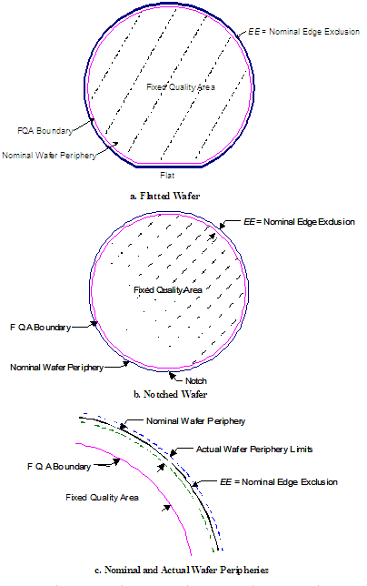
Edge exclusion for GaN thickness uniformity: |
1mm |
|
3.13 |
XRD FWHM: |
< 350" for (102) and < 300" for (002) |
|
3.14 |
Si doping level: |
5E18 - 1E19cm-3 |
|
3.15.1 |
Sheet Resistance: |
<50Ω/sq |
|
3.15.2 |
Resistivity: |
<20mΩ-cm |
|
3.16 |
Surface roughness: |
< 12nm Ra (3 profilometer scans - 1mm length each) |
|
3.17 |
Bow (measure with 1 mm edge exclusion) |
<50um |
|
3.18.1 |
Edge exclusion for defects: |
2mm |
|
3.18.2 |
Defects: Particles and Pits |
< 200 per 2-inch wafer |
|
3.18.3 |
Defects: Large Defects > 50um |
0 per 2-in wafer |
|
3.19 |
Fishscale |
not allowed |
|
SEMI Standards |
|
|
M1 |
Specifications for Polished Single Crystal Silicon Wafers |
|
M12 |
Specification for Serial Alphanumeric Marking of the Front Surface of Wafers |
|
M65 |
Specifications for Sapphire Substrates to Use for Compound Semiconductor Epitaxial Wafers |
|
MF26 |
Test Method for Determining the Orientation of a Semi-conductive Single Crystal |
|
MF523 |
Practice for Unaided Visual Inspections of Polished Silicon Wafer Surfaces |
|
MF533 |
Test Method for Thickness and Thickness Variations of Silicon Wafers |
|
MF534 |
Test Method for Bow of Silicon Wafers |
|
MF657 |
Test Method for Measuring Warp and Total Thickness Variation on Silicon Wafers by Noncontact Scanning |
|
MF671 |
Test Method for Measuring Flat Length on Wafers and Other Electronic Materials |
|
MF847 |
Test Method for Measuring Crystallographic Orientation of Flats on Single Crystal Silicon Wafers by X-ray Techniques |
|
MF928 |
Test Method for Edge Contour of Circular Semiconductor Wafers and Rigid Disk Substrates |
|
MF1152 |
Test Method for Dimensions of Notches on Silicon Wafers |
|
MF1530 |
Test Method for Measuring Flatness, Thickness, and Total Thickness Variation on Silicon Wafers by Automated Non-contact Scanning |
|
MF2074 |
Guide for Measuring Diameter of Silicon and Other Semiconductor Wafers |
|
ANSI/ASQC Z1.4 |
Sampling Procedures and Tables for Inspection by Attributes |
|
E122 |
Standard Practice for Calculating Sample Size to Estimate, with Specified Precision, the Average for a Characteristic of a Lot or Process |
|
H 0611 |
Methods of measurement of thickness, thickness variation and bow of silicon wafer |
|
H 0614 |
Visual inspection for silicon wafers with specular surfaces |
Source:PAM-XIAMEN
If you need more information about GaN/sapphire wafers, please visit:http://www.qualitymaterial.net or send us email at sales@qualitymaterial.net.