> News > Lattice location determination of trace nitrogen dopants in semiconductor silicon carbide (SiC)
The superconducting X-ray detector developed by AIST, used to identify N dopants at a very low concentration in SiC (left) and SC-XAFS installed at a beam line of Photon Factory, KEK (right)
AIST researchers have developed an instrument for X-ray absorption fine structure (XAFS) spectroscopy equipped with a superconducting detector. With the instrument, the researchers have realized, for the first time, local structure analysis of nitrogen (N) dopants (impurity atoms at a very low concentration), which were introduced by ion plantation in silicon carbide (SiC), a wide-gap semiconductor, and are necessary for SiC to be a n-type semiconductor.
Wide-gap semiconductor power devices, which enable reduction of power loss, are expected to contribute to the suppression of CO2 emissions.To produce devices using SiC, one of the typical wide-gap semiconductor materials, introduction of dopants by ion plantation is necessary for the control of electrical properties. The dopant atoms need to be located in the particular lattice site in a crystal. However, there has not been a microstructure analysis method. SC-XAFS was used to measure the XAFS spectra of the N dopants at a very low concentration in the SiC crystal, and the substitution site of the N dopants was determined by comparison with a first-principle calculation. In addition to SiC, SC-XAFS can be applied to wide-gap semiconductors such as gallium nitride (GaN) and diamond, magnets for low-loss motors, spintronics devices,solar cells, etc.
The results will be published online in Scientific Reports, a scientific journal published by the Nature Publishing Group, on November 14, 2012 (UK time).
SiC has a band gap larger than that of general semiconductors and possesses excellent properties including chemical stability, hardness, and heat resistance. Therefore, it is expected to be a next-generation energy-saving semiconductor which can function in a high-temperature environment. In recent years, large single-crystal SiC substrates have become available and devices such as diodes and transistors appeared on the market; however, doping, which is necessary to produce devices with the semiconductor, is still imperfect, preventing SiC from fully utilizing its intrinsic energy-saving properties.

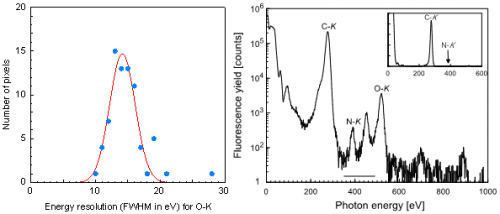
Figure 1: (a) The energy resolution of the superconducting X-ray detector with respect to the characteristic X-ray of oxygen (b) An example of the detection of the N dopant in a very low concentration in SiC The strong peak of abundant C in SiC and the weak peak of N are distinguishable. In the insertion in (b), the vertical axis is in a linear scale. It is clear that N exists in a very low concentration.
Doping is a process in which a small amount of impurity is introduced (for substitution) into a crystal lattice site to form a semiconductor with electrons playing a major role in electrical conduction (n-type semiconductor) or with holes playing a major role in electrical conduction (p-type semiconductor). SiC is a compound, and thus has a complex crystal structure, which means that doping into SiC is by far more difficult than doping into silicon (Si). Since dopants should be light elements such as boron, N, aluminum, or phosphorus, there was no measurement method to study at which site in the SiC crystal they are located, namely the Si site or the carbon (C) site. Although transmission electron microscopy can visualize atoms, it is difficult to distinguish a trace light element from light elements constituting the matrix material. To determine dopant lattice sites, XAFS spectroscopy is effective. X-ray fluorescence analysis allows to measure XAFS spectra of a specific element in matrices, and reveals the atomic arrangement and the chemical state around the element. So far, however, it has been impossible to distinguish the characteristic X-ray of a light element at a very low concentration from those of the matrix elements, Si and C. The lack of the analysis method has hindered the development of wide-gap semiconductors.
AIST has been developing advanced measurement technologies for industrial research and scientific studies, making them available for public use, and standardizing them. As a part of these efforts, SC-XAFS using a superconducting measurement technology was completed in 2011. N has an atomic number larger than C by one. The energy of its characteristic X-ray is 392 electron volts (eV); the difference from that of C, 277 eV, is only 115 eV. Although the energy resolution of the latest semiconductor X-ray detectors is 50 eV or so, which is smaller than the difference, at this resolution, while light elements can be distinguished if they exist in a large mount, it is not possible to distinguish a light element at a very low concentration, such as dopants. In contrast, the superconducting X-ray detector developed by AIST has the resolution that exceeds the theoretical limitation of semiconductor X-ray detectors. Therefore, it is possible to measure the XAFS spectrum of the N dopant in SiC using the superconducting detector (AIST TODAY, Vol. 12, No. 3).

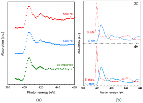
Figure 2: (a) The XAFS spectrum of the SiC wafer without heat treatment immediately after the N ion plantation at 500 °C, and those of the SiC wafer heat-treated at high-temperatures after the ion implantation (b) The XAFS spectra assumed from the first-principle calculations with the Si site replaced by N and with the C site replaced by N. The experiment data agrees with the result of the calculation on the assumption that the C sites were replaced in the comparison of (a) the measured spectra and (b) the calculated spectra for the 3C and 4H polytypes, which were two typical crystal structure SiC.
This SC-XAFS is installed in the BL-11A beam line of Photon Factory, KEK and is available to the public since 2012 in the projects such as the AIST advanced equipment sharing innovation platform and the microstructural analysis platform in the nanotechnology platform project. Only AIST and Advanced Light Source in the USA have this kind of advanced measurement instrument; and only AIST has developed a superconducting detector, the key of the analytical instrument. ITC developed the ion injection technology and the heat treatment technology applicable to SiC and supplies samples to users.
Figure 1 (a) shows a histogram of the energy resolution of each element of the superconducting array detector. At a maximum resolution of 10 eV, which exceeds the limit of 50 eV of semiconductor detectors, the detector can distinguish a trace amount of N from the matrix C in a large quantity (Fig. 1 (b)), thus enabling the acquisition of XAFS spectra with accuracy usable for comparison with first-principle calculation (Fig. 2 (b)).
The SiC wafer into which the N dopant was introduced by ion plantation at a temperature of 500 °C and the wafers heat-treated at 1400 °C or 1800 °C after the ion plantation were subjected to the measurement of XAFS spectra (Fig. 2 (a)). The result of this experiment agreed with the first-principle calculation with FEFF, in which it was assumed that N atoms were located in the C sites (Fig. 2 (b)). Thus, it was confirmed that most of N atoms were located in the C sites immediately after the ion plantation. It was empirical knowledge that ion plantation at a temperature as high as 500 °C was necessary for the doping to SiC, the reason for which, however, was unknown. The reason revealed in the present study is that it is necessary to locate N in the C sites before heat treatment at high temperature. Moreover, according to the spectrum in the region lower than 400 eV, it is presumed that a chemical bond is formed between C and N in a disordered crystal state immediately after the ion plantation. As the crystal disorder resolves as a result of the heat treatment at high temperature, this chemical bond breaks, leaving only the chemical bond of N and Si, which is preferable for the doping. As described here, it is revealed that the doping to SiC is complex and requires a completely different method from that for the doping to Si, in which the lattice site substitution can be realized by heat treatment after ion implantation at room temperature.
It is now possible to determine the lattice site of the trace N dopant introduced in SiC; no such measurement was possible hitherto. Furthermore, the state of the chemical bonds of the N dopant with the base materials, Si and C, is revealed. By combining SC-XAFS and the first-principle calculation, it is proved that the detection and microstructural analysis of a trace amount of the light elements in a crystal is possible, both of which were impossible until now.
The developed technology is expected to contribute to the optimization of the doping process of SiC semiconductors. Besides SiC, SC-XAFS will be applied to the analysis of other wide-gap semiconductors, magnetic materials, etc.; their functions depend on trace light elements. Furthermore, improvement will be attempted in the resolution of the superconducting X-ray detector and the capability of the detection of a trace amount of light elements, thus expanding the range of the impurity concentrations covered by SC-XAFS.
Explore further:writing graphene circuitry with ion ‘pens’
Journal reference:Scientific Reports
Provicded by:Advanced Industrial Science and Technology
Source:PHYS
For more information, please visit our website:www.qualitymaterial.net,send us email at angel.ye@powerwaywafer.com or powerwaymaterial@gmail.com.