Home > News > Epitaxial growth of homogeneous single-crystalline AlN films on single-crystalline Cu substrates

Epitaxial growth of homogeneous single-crystalline AlN films on single-crystalline Cu substrates

 Highlights


Single-crystalline AlN films have been grown on single-crystalline Cu substrates.

High thickness homogeneity AlN films have been achieved.

Crack free AlN films have been grown single-crystalline Cu substrates.

The as-grown ∼321 nm thick AlN films are only with a compressive strain of 0.48%.  
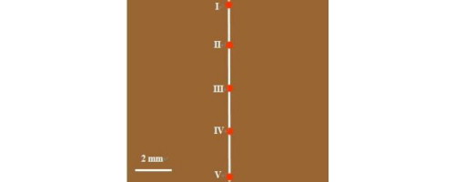


The homogeneous and crack free single-crystalline AlN thin films have been epitaxially grown on single-crystalline Cu (1 1 1) substrates with an in-plane alignment of AlN [11–20]//Cu [1–10] by pulsed laser deposition (PLD) technology with an integrated laser rastering program. The as-grown AlN films are studied by spectroscopic ellipsometry, field emission scanning electron microscopy (FESEM), atomic force microscopy (AFM), polarized light microscopy, high-resolution X-ray diffraction, and high-resolution transmission electron microscopy (HRTEM). The spectroscopic ellipsometry reveals the excellent thickness uniformity of as-grown AlN films on the Cu (1 1 1) substrates with a root-mean-square (RMS) thickness inhomogeneity less than 2.6%. AFM and FESEM measurements indicate that very smooth and flat surface AlN films are obtained with a surface RMS roughness of 2.3 nm. The X-ray reflectivity image illustrates that there is a maximum of 1.2 nm thick interfacial layer existing between the as-grown AlN and Cu (1 1 1) substrates and is confirmed by HRTEM measurement, and reciprocal space mapping shows that almost fully relaxed AlN films are achieved only with a compressive strain of 0.48% within ∼321 nm thick films. This work demonstrates a possibility to obtain homogeneous and crack free single-crystalline AlN films on metallic substrates by PLD with optimized laser rastering program, and brings up a broad prospect for the application of acoustic filters that require abrupt hetero-interfaces between the AlN films and the metallic electrodes.    

Graphical abstract

Graphical abstract

Keywords

  • AlN
  • Cu (1 1 1) substrates
  • Pulsed laser deposition
  • Laser rastering program
  • Hetero-interfaces
  •  
  •  
  •  

    Source:Sciencedirect


  • If you need more information about sic wafer, please visit:http://www.qualitymaterial.net or send us email at sales@qualitymaterial.net