1. Introduction
Because of their unique properties, such as high hardness, good corrosion resistance, and excellent chemical stability, SiC materials are widely used for tribological applications in extreme conditions . However, the friction and wear coefficients of SiC materials are unacceptably high in unlubricated conditions . To improve the tribological properties, carbon coatings such as diamond and diamond like carbon (DLC), are usually coated on such materials using chemical vapor deposition (CVD) process and . Although the CVD process is well established, the search for new methods for depositing carbon films continues. A promising method for coating carbon films on SiC termed the “carbide-derived carbon” or CDC process is greatly attractive in recent years . In this method, SiC is treated in a chlorine-containing gas mixture at high temperature, and the Si atoms preferentially react with Cl2 and leave the system in the form of SiCl4 The left carbon atoms rearrange themselves and form a smooth carbon film that is intimately bonded to the underlying SiC substrate. Compared with CVD process, the CDC process can easily produce a thick carbon layer (above 100 um) at a high rate and .
The CDC with unique nanostructure possesses many attractive physical, mechanical, and tribological properties. In particular, it is reported in recent studies that the CDC coating can afford very low friction and wear to improve the tribological performance of the carbides. Specifically, this coating can provide a friction coefficient of 0.03–0.3 and wear rate of 10− 9–10− 7 mm3/N·m depending on the chlorination process and friction test conditions and. Surprisingly, the CDC coating with high porosity (i.e.> 57.2% for β-SiC) shows excellent tribological properties under dry friction condition. However, unpublished studies in our group confirm that the CDC coating is helpless in lubricating for SiC materials under some conditions, including high temperature (i.e. at 300 °C), water or oil lubrication and high load. The lubrication failure is attributed to the high porosity and the low strength of CDC coating. Further surface modification to improve the density and strength of CDC coating is urgent for extensive tribology application. Although there is little pertinent research on such work to date, some information can still be obtained in some literature. Grannen and Chang deposited diamond films from fluorocarbon gases in microwave plasma on SiC and WC substrates without any pretreatments. The proposed growth mechanism suggests that the surface carbon layer formed by the etching of carbide substrates with fluorine atomic favors the nucleation of diamond. It is reported that ultrananocrystalline diamond (UNCD) could also be deposited on the CDC films using microwave plasma CVD reactor and the tetrahedrally bonded carbon in the CDC films is suggested as a good seed for UNCD deposition .
Accordingly, we attempt to prepare a novel dual-layer carbon coating on 6H-SiC wafers using CDC technique with subsequent CVD process in the present work. According to our considerations, the CDC layer which is formed by chlorination of SiC acts as a seed and intermediate layer for subsequent deposition. The CVD process is operated in a same reactor using CCl4 as carbon source. We used Raman spectroscopy, X-ray photoelectron spectroscopy (XPS), atomic force microscopy (AFM) and field emission scanning electron microscopy (SEM) to determine the microstructure and chemistry of CDC and CVD films. And friction and wear properties of the CDC and dual-layer film are discussed. It is expected that this dual-layer film can provide better lubrication for SiC materials in many applications.
2. Experimental section
2.1. Film preparation
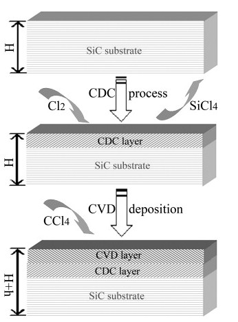
The dual-layer film was synthesized by pre-chlorination of single crystalline 6H-SiC wafer with subsequent chemical vapor deposition (CVD) using CCl4 as precursor. The n-type 6H-SiC wafer (10 × 10 mm2) with polished Si-face was purchased from TianKe Blue Semiconducter Co. Ltd (Beijing, China), with nominal cut-off angle of about 0–5°. The as-received SiC wafers were etched in dilute HF acid (40% solution) for 5 min to remove a SiO2 layer, and ultrasonically cleaned in acetone bath for treatment. The schematic process to synthesize the dual-layer film was demonstrated in Fig. 1. Both the CDC process and CVD deposition were carried out in a tube furnace in turn. The CDC process was described in detail elsewhere . In our experiments, the CDC layer was fabricated by chlorination of SiC in a gas mixture (Cl2 at a flow speed of 2 ml min− 1 + Ar at a flow speed of 98 ml min− 1) at 1000 °C for 10 min. The Si was preferred to react with Cl2and removed away in the form of volatile SiCl4. The surface of SiC was converted into CDC and the shape of the sample stayed unchanged, as demonstrated in Fig. 1. Once the CDC process was finished, the Cl2 flow was stopped immediately. Subsequently, the CCl4 was evaporated at 60 °C and introduced into reaction region with 50 ml min− 1 Ar flow. The carbon derived from pyrolyzing of CCl4 at 1000 °C nucleated and grew on top of CDC layer to form the CVD layer. The duration for CVD deposition was 2 h. The two principal chemical reactions taking place in the process included
SiC+22Cl→SiCl4+C
which is thermodynamically allowed, with a Gibbs energy of ∆G = − 434.1 kJ/mol at 1000 °C, and
CCl4→C+Cl2
which is also thermodynamically allowed, with a Gibbs energy of ∆G = − 36.672 kJ/mol at 1000 °C. The carbon produced by reaction (1) formed the CDC layer, while reaction
(2) formed the CVD layer. As a result, the dual-layer carbon film composed of sub-layer of CDC and top layer of CVD carbon was synthesized. Moreover, single CDC film was also synthesized for comparison. The process parameters were the same to those in CDC process for dual-layer film preparation.
Fig. 1. Schematic fabrication process for the dual-layer carbon film. The processes were carried out in a silica tube furnace at 1000 °C. The surface of SiC was converted into CDC by etching in a chlorine-containing gas mixture. The shape of the sample stayed unchanged. The CVD layer was prepared by pyrolyzing CCl4 on top surface of CDC layer and increased the sample thickness.
2.2. Characterization
Raman spectroscopy is a standard non-destructive analysis tool for characterization of various carbon materials. The CDC and the dual-layer films were studied on a Horiba HR800 Raman system with an Ar laser excitation wavelength of 532 nm. This system is also equipped with a charge couple device (CCD) detector and an optical imaging for focusing the laser at a micro-region. The Raman spectra were collected in the range between 600 and 2000 cm− 1 for 60 s. X-ray photoelectron spectroscopy (XPS) was used to analyze the surface composition and chemical nature of the CDC layer and the dual-layer film. The XPS measurement was performed on PHI-5702 multifunctional photoelectron spectrometer, using Al–Ka X-ray (250 W) as the excitation source. No pre-treatment on the samples was conducted. Survey spectra with energy step of 0.4 eV and core level photoelectron lines C1s, O1s, Cl2p and Si2p with energy step of 0.125 eV were recorded. In order to investigate the surface topography evolvement, atomic force microscopy (AFM) was carried out with a Nanoscope IIIA Multimode apparatus (Veeco Instruments) under ambient conditions (relative humidity ~ 45%, temperature ~ 26–28 °C). AFM was performed in the tapping mode using rectangular silicon cantilevers with spring constant of ~ 40 Nm− 1 and typical resonance frequencies between 250 and 300 kHz. Field emission scanning electronic microscopy (FESEM, JSM-6701F) was also employed to observe the surface microstructure.
2.3. Friction test
Friction and wear behaviors of SiC, CDC layer and dual-layer film were contrastively studied on a UMT-2MT tribo-meter (CETR, USA) with a ball-on-disk configuration in ambient conditions (temperature of 27 °C and relative humidity of 45%). The Si3N4 and steel balls with diameter of 3 mm made oscillating movement (5 mm in amplitude) on the top of the samples for 30 min. The test conditions were 1 N in load and 20 mm s− 1 in sliding speed. The friction coefficients were recorded by the tribo-meter.
3. Results and discussion
3.1. Raman spectrum
For the perfectly ordered graphite, the first-order Raman spectrum recorded in the near-infrared and visible light regimes shows only one peak around 1580 cm− 1, whereas disordered amorphous carbon generally exhibits two peaks: the so-called G-band at ~ 1580 cm− 1and the so-called D-band (disorder induced (D)) at ~ 1350 cm− 1, which is associated with the double-resonance Raman mechanism. The positions of D- and G-bands, their relative intensity ratio (ID/IG), and their full widths at half maximum (FWHM) can be used to study the structural information of the carbon materials. Fig. 2 presents the Raman spectra of SiC substrate, CDC layer, and dual-layer film to investigate the structure evolvement. The Raman spectrum of SiC has several peaks in the range of 800–2000 cm− 1. The strongest peak ~ 968 cm− 1 is the longitudinal (LO) optical phonon of SiC, while the peak ~ 782 cm− 1 is the transversal optical (TO) phonon. The positions of D- and G-bands for CDC layer situate at ~ 1337 cm− 1 and ~ 1606 cm− 1, respectively, being different from the specific values for graphite (~ 1350 cm− 1 and ~ 1580 cm− 1). Moreover, the D- and G-bands for CDC layer are greatly broadened and cannot be fitted with two Gaussians profiles. As we know, the G-peak appears due to the in-plane bond-stretching motion of pairs of sp2 bonded C atoms in graphitic compounds whatever is their stacking order or their crystallite size. The broadening and shifting to high wavenumbers of the G-band can be interpreted as an increase in bond angle disorder or the ultrasmall crystal size . Alternatively, the internal stress induced by the nonuniformity of the crystalline structure and the mismatch between CDC and SiC substrate leads to peak broadening and up-shifting in Raman spectrum of CDC layer. Unfortunately, the origin of the D-band shifting toward smaller wavenumbers is unclear. However, the presence of broad D-band further demonstrates the disorder structure. Its large FWHM implies a large distribution of sp2 bonded clusters with different ring sizes in the CDC layer. 2 + 2 Gaussian profiles can be used to fit the Raman spectrum to calculate the integrated intensity ratio of D- and G-bands (ID/IG ≈ 1.70). According to the Tuinstra and Koenig (TK) equation and, the in-plane correlation length (La) or the average size of the graphite sheets in the CDC layer is estimated to be about 2.92 nm.
Fig. 2. Raman spectra of SiC substrate, CDC layer and dual-layer film. The Raman features of dual-layer film are similar to that of the CDC layer, although the position of D-band shifts to the higher wavenumber.
The Raman features of the CVD layer are similar to that of the CDC layer, although the position of D-band shifts to the higher wavenumber at ~ 1354 cm− 1. Since the CVD carbon nucleates and grows on the top of CDC layer, top layer may copy the structure of CDC layer in some extent and therefore their Raman feature is similar. The up-shifted D-band of CVD layer may be attributed to the increased size of the graphite microcrystalline. It is also necessary to note that the densification of the CVD layer and the reduced internal stress may lead to the difference in Raman spectrum. The Raman spectrum of the CVD layer was also fitted with 2 + 2 Gaussian mode. The integrated intensity ratio (ID/IG) reduces to 1.32, corresponding to an increased La of 3.75 nm compared to CDC layer.
3.2. XPS analysis
The XPS measurements were carried out aiming to determine the surface composition and chemical nature for SiC, CDC layer and dual-layer film, as demonstrated in Fig. 3. It is mentioned that oxidizing of silicon carbide surface can easily take place even at room temperature . The oxygen peak in the survey spectrum may correspond to the contaminated oxygen or the oxidation of SiC surface (Fig. 3a). Surface analysis of the CDC layer reveals that it does not consist purely of carbon, but that it still contains O, Si and Cl components. The oxygen is related to the oxidation of CDC as well as physical adsorption of O2 and H2O molecular due to the highly porous structure. Surprisingly, the Si is identified within the CDC layer. Zinovev et al. reported that the silicon maybe exist in oxidized forms of silicon, i.e. SiO2, which derives from the oxidation of the escaped SiCl4 gas with trace oxygen. The surface atomic concentration of Cl in the CDC layer by XPS analysis is about 5.5 at.%. Since the CDC layer results from selective etching of Si atoms in SiC by Cl2, some of the Cl2 is likely retained in the CDC layer in atomic or bonded form . For the survey spectrum of dual-layer film, the surface composition is characterized by mainly the presence of C and O components with minor contents of Si (6.5 at.%) and Cl (1.8 at.%). The attenuation of Si and Cl signals does not indicate that they are removed in subsequent CVD process, but their signals are covered by the top layer with increasing thickness.
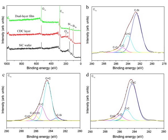
Fig. 3. XPS results showing [a] the survey spectra, the corresponding core levels C1s of [b] SiC substrate, [c] CDC layer, and [d] dual-layer film. All C1s core levels are fitted with Gaussian mode.
More detailed information about the surface chemistry can be obtained from the analysis of the core level C1sspectra. Fig. 3b–d shows the C1s core levels of SiC, CDC layer and CVD layer and their line shape fits. The C1s peak on SiC demonstrates that the composition is dominated by the binding energy of C–Si (282.7 eV) with C═C (284.3 eV), C–C (285.0 eV), and C―O (286.1 eV) at the high binding energy (Fig. 3b). The C1speak of CDC can be fitted by five components with binding energies of 284.4, 285.3, 286.2, 287.2, and 283.0 eV. The first component is attributed to the sp2 bonded carbon, whereas the second one is attributed to the sp3 coordinated bonds in amorphous carbon and . The component at 287.2 and 283.0 eV is assigned to C═O bonded carbon and C―Si bond, respectively. The component with bonding energy of 286.2 eV is attributed to C―Cl or C―O bond. In Fig. 3d, the C1s peak of the dual-layer film is fitted by four components with the binding energy of 284.3, 285.1, 286.1, and 287.0 eV. Similar to that of the CDC layer, the two contributions at low binding energy are assigned to the sp2 and sp3 C. The components at 286.1 and 287.0 eV should be attributed to C―O and C═O bond, respectively.
From the XPS analysis, both the CDC and the dual-layer film mainly consist of sp2 bonded carbon with a small mixture of sp3 carbon, C―O, and C═O. However, the effect of surface chemical nature of CDC layer under the top layer cannot be studied by XPS. Indeed, there are many voids, defects, and active atomic and/or molecular sites, which may contain dangling or unsatisfied σ-bonds within the CDC film (especially near the top). Before the CVD process, such active sites are passivated by physical interaction (i.e. physical adsorption) and formation of metastable chemical bonds, e.g. the C―Cl bond. In other words, the surface of the CDC layer is highly active, which can act as a “seedbed” for nucleation and growth of the top layer.
3.3. Surface morphology
Fig. 4 shows the AFM images and corresponding 3D profiles of SiC wafer, CDC layer and dual-layer film, indicating surface morphology evolution in the process. The as-received SiC surface in Fig. 4a and b is characterized by highly uniform and flat terraces. The surface roughness RMS (root mean square roughness) is evaluated as 0.22 nm. The step direction and terrace width are determined by the incidental disorientation of the substrate surface with respect to the crystallographic (0001) plane . The step height is smaller than that of the dimension of the 6H-SiC unit cell in the direction perpendicular to the surface (c axis), which may resulted from the silicon oxide layer. The morphology of the CDC layer prepared by chlorination is shown inFig. 4c and d. The SiC surface undergoes significant modification: it is now covered with numerous nanopores up to 100 nm in width, and the original are disappeared. The formation of CDC is accompanied by substantial changes in the morphology, leading to a considerable increasing surface roughness of 1.46 nm. As a consequence of chlorination, the CDC layer possesses a nanoporous structure and an increasing specific surface area on the surface and. The nanopores can easily capture the carbon species from the gas phase for the subsequent CVD process, which benefits the nucleation and growth of the CVD layer. After the CVD process, the surface morphology is characterized by spherical or ellipsoidal particles, as shown inFig. 4e and f. The size of carbon particles is up to approximately 3 μm in diameter, and the surface roughness is substantially increased to 54.68 nm in RMS.
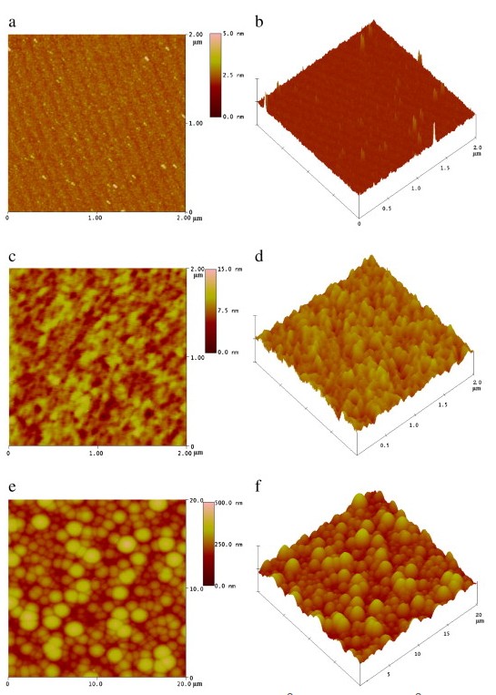
Fig. 4. AFM images of [a] as-received SiC wafer [2 × 2 μm2], [c] CDC layer [2 × 2 μm2], [e] the dual-layer film [20 × 20 μm2], and their corresponding 3D profiles [b], [d], and [f]. The surface roughness [RMS] increases from 0.22 nm for SiC to 1.46 nm for CDC, and the roughness of dual-layer film is the largest of 54.68 nm.
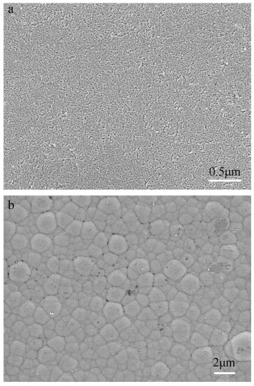
The surface microstructures of the CDC layer and the dual-layer film are also investigated by FESEM as shown in Fig. 5. As the CDC layer is formed by selective etching of Si from SiC, the surface is characterized of a highly porous structure mainly consisted of numerous nanoscale pores and a corresponding large specific area of the CDC layer (Fig. 5a). Assuming all the Si atoms are removed from SiC and no volume change occurs, a large pore volume of 57.3% will be obtained. Such a unique microstructure of nanopores as well as the surface chemical activity should promote the nucleation and growth of CVD layer. Fig. 5b shows the microstructure of the CVD layer. The whole surface is uniformly covered with quasi-spherical carbon particles with size in submicrometer scale, with accordance to the observation by AFM (Fig. 4c and d).
Fig. 5. The high revolution SEM micrographs of [a] CDC layer and [b] dual-layer carbon film.
3.4. Tribological property
The tribological behaviors of SiC wafer, CDC, and dual-layer film are contrastively investigated to evaluate the potential lubrication. Fig. 6a and b shows the friction coefficient as a function of sliding time of the samples sliding against Si3N4 and steel in room air, respectively. After a run-in process of about 500 s, the friction coefficient of SiC wafer against Si3N4 is steady at 0.80, which is the typical value of SiC ceramic in open air. Meanwhile, the friction coefficient curve fluctuates rather heavily during testing. The friction coefficient of the CDC layer greatly reduces to 0.25, showing an improved tribological behavior compared to SiC. When sliding against Si3N4, the friction coefficient of the dual-layer film is further reduced to 0.15. Differently, the friction coefficients of the CDC layer and the dual-layer film against steel ball are higher than Si3N4. Specifically, the friction coefficient of the CDC layer drastically fluctuates in initial process and the average value is above 0.3, while that of the dual-layer film is very steady and slightly increases to 0.17.
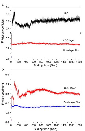
Fig. 6. Friction coefficient as a function of sliding time of the SiC wafer, the CDC layer, and the dual-layer film sliding against [a] Si3N4 and [b] steel in room air.
From the tribological results, we can conclude that the Si3N4 is the preferred dual material over the steel whenever sliding against the CDC layer or the dual-layer film. The steel is easily worn because of its much lower hardness than Si3N4. The debris from the steel retained in the contact surface can lead to severe abrasive wear. Moreover, chemical corrosion and adhesive interaction prefer to occur in the contact surface to increase friction when sliding against steel. Whereas, such negative effects are attenuated when against Si3N4 ball because of its high hardness and chemical inertness. Additionally, the dual-layer film shows advantages over the CDC layer in friction reduction. As aforementioned, the surface of the CDC layer is highly active with many dangling bonds, unsatisfied σ-bonds, and unstable chemical bonds (the C―Cl, for instance) . The presence of such bonds at sliding contact interfaces is undesirable as they can easily cause adhesive interactions during sliding motion. In addition, hard particles of SiO2 in the CDC layer can increase the friction in the form of abrasion. For the dual-layer film, the active bonds are effectively eliminated by highly energetic carbon atoms generated in pyrolyzing of CCl4. Moreover, the concentration of Cl atomics on the surface is greatly reduced, which can be seen from the XPS results. As a result, the dual-layer film shows an improved tribological behavior compared with the CDC layer.
4. Conclusions
A dual-layer carbon film was successfully synthesized by carbide-derived carbon process and subsequent chemical vapor deposition. The dual-layer film is composed of a CDC layer formed by chlorination of SiC and a CVD layer formed by pyrolyzing the CCl4 at high temperature. Due to the selective removal of Si from SiC, the as-received CDC layer is highly porous in structure and contains many dangling bonds and unsatisfied σ-bonds on the surface. By AFM and FESEM observation, the porous structure of CDC layer is characterized with numerous nanopores that can benefit the surface capturing carbon containing species from gas mixture. On the other hands, the as-received CDC surface is chemically active, so the pyrolyzed carbon atoms are readily bonded to the surface. In short, the CDC layer serves as a seed and intermediate layer for the subsequent CVD carbon deposition. The dual-layer film shows a typical amorphous structure, exhibiting D- and G-bands in Raman spectrum at ~ 1354 and ~ 1605 cm− 1, respectively. The preliminary tribological study demonstrates that the dual-layer film outperforms the single CDC layer in lubricating SiC substrate. It is expected that this dual-layer film will find great potential in lubrication for SiC-based moving components. In the future, it is necessary to further understand the growth mechanism, control the structure and improve the properties of this dual-layer film by optimizing the process parameters.
Source: Elsevier B.V.
If you need more information about Preparation and characterization of a dual-layer carbon film on 6H-SiC wafer using carbide-derived carbon process with subsequent chemical vapor deposition, please visit:http:http://www.qualitymaterial.net/ or send us email at sales@qualitymaterial.net