Low dark current and internal gain mechanism of GaN MSM photodetectors fabricated on bulk GaN substrate
Metal-semiconductor–metal ultraviolet photodetectors are fabricated on low-defect-density homoepitaxial GaN layer on bulk GaN substrate. The dislocation density of the homoepitaxial layer characterized by cathodoluminescence mapping technique is ∼5 × 106 cm−2. The photodetector with a high UV-to-visible rejection ratio of up to 1 × 10⁵ exhibits a low dark current of <2 pA at room temperature under 10 V bias. The photo-responsivity of the photodetector gradually increases as a function of applied bias, resulting in a photodetector quantum efficiency exceeding 100% at above medium bias. The photo-responsivity also shows a dependence on the incident optical power density and illumination conditions. The internal gain mechanism of the photodetector is attributed to photo-generated holes trapped at the semiconductor/metal interface as well as high-field-induced image-force lowering effect.
Research highlights
► MSM UV photodetectors are fabricated on low-defect-density homoepitaxial GaN layer.
► The photodetector exhibits ultra-low dark current and high UV/visible rejection ratio.
► The internal gain is attributed to hole trapping at interface and image-force lowering effect.
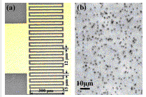
Fig. 1. (a) Photograph of an interdigitated GaN MSM photodetector and (b) panchromatic CL mapping image of the homoepitaxial GaN layer grown on bulk GaN substrate.
Source: Solid-State Electronics