Bulk micromachining of SiC substrate for MEMS sensor applications
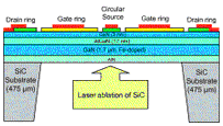
We present a non-conventional bulk micromachining process of SiC substrate directed to fabrication of MEMS sensors based on III-nitrides (III-N) material systems for harsh environment. They consist of AlGaN/GaN/SiC high electron mobility transistors (HEMTs). The key issue is here the creation of appropriate diaphragms necessary to verify the multi-sensing properties of such MEMS sensors. The backside of the SiC substrate must be selectively removed in the defined areas. Considering the extremely high chemical stability of SiC, for the deep patterning we propose a method which uses femtosecond (FS) laser ablation combined with deep reactive ion etching (DRIE). The different writing strategies in order to improve the texturing of SiC are also discussed. Electrical parameters comparison of the fabricated devices on both Si and SiC substrates were performed. Four times higher values of maxima of drain current for HEMTs on AlGaN/GaN/SiC were measured.
Highlights
► Laser ablation is a usable fabrication step of MEMS for harsh environment.
► The extreme chemical inertness of SiC is circumvented.
► The problem with lack of an etch stop layer can be solved.
► The range of pressure sensitivity of the sensors can be also modified.
Fig. 1. Cross-section view of the proposed MEMS sensor device based on C-HEMT.
Source: Microelectronic Engineering